
How is Solder Mask Applied in Microwave Printed Circuit Boards (PCBs)?
Solder Mask Applied in Microwave Printed Circuit Boards (PCBs)
Solder mask is one of the most important procedures in Printed Circuit Boards (PCBs). It protects the copper traces and holes from oxidation and corrosion during production and assembly. It also provides an efficient foundation for soldering components to the bare copper PCB. In addition, it improves aesthetics and allows for easy inspection.
During the PCB fabrication process, the mask is applied as a thin layer of polymer-resist material covering the bare copper traces and pads. The solder mask color is specified in the Gerber file along with all other electrical and mechanical layers. The mask can be either dry film or liquid, and it is typically applied with a photolithography imaging process or through a curtain coating system.
Photolithography involves using a laser plotted image to expose the microwave pcb panel with dry mask materials. The panel is exposed to UV light except for the areas that will be soldered, allowing the unexposed solder mask to harden. The laser also creates openings in the mask that will define the copper pads and holes on the finished board.
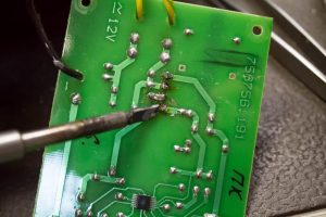
How is Solder Mask Applied in Microwave Printed Circuit Boards (PCBs)?
Dry film photoimageable solder mask uses a similar process to apply the resist, but instead of applying the mask as an ink, manufacturers roll it out in sheets and vacuum laminate it to the PCB. The panels are then etched and cleaned before being imaged with a UV laser, exposing the mask to UV only where needed. This method is usually faster and less expensive than liquid mask processing.
Liquid photoimageable solder masks (LPISM) and epoxy can be applied in an ink form, which can be sprayed or silk-screened onto the circuit board. These types of masks are less expensive than dry film but they are susceptible to flaking, which can affect performance. Liquid masks can be customized by mixing in dye during manufacturing to achieve different colors.
There are a number of issues that can arise during the application process, including voids, scratches, and delamination. Voids leave unprotected copper traces vulnerable to oxidation, which can result in solder bridges or shorts. Scratches can cause abrasion that disrupts the mask surface and exposes the copper, and delamination can occur due to thermal stresses or poor adhesive properties.
Despite these problems, the majority of solder mask defects can be corrected manually with ink pens or brushes. Larger defects may require mask stripping and reapplication. The underlying copper is then cleaned and prepared for plating, which can be done with immersion gold or electroless nickel.
The most common color for solder mask is green, which has been shown to have the smallest solder dam, which allows the most efficient copper movement during soldering. Other colors, however, can be used based on inspection considerations or aesthetic preferences. The choice of color depends on a variety of factors, including the type of mask, its thickness, and its resistance to high temperatures. It is also important to consider the impact of environmental conditions on the mask color, as well as its chemical characteristics and compatibility with various metallization processes.